
Reference Number
A198993
描述
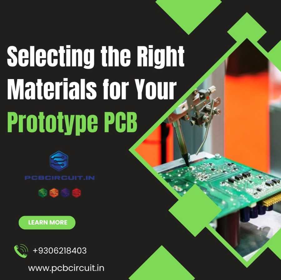
The process of prototype PCB manufacturing begins with the design phase, where a schematic of the circuit is translated into a PCB layout using specialized software like Eagle, Altium Designer, or KiCad. Once the design is complete, it is converted into a set of files that define the board’s physical characteristics, such as traces, vias, and component placements. Prototype PCBs are typically produced in small batches (often between 1-10 units), allowing for quick iteration and testing.
国家
India
州/地区/省
Telangana
城市
Hyderabad
邮政编码
500055
地址
Bhagya Lakshmi Colony, 709/5/3/10/P, Subhash Nagar

- 138 观点
-
查看二维码

- Report Listing Cancel Report
-
- Current rating: 0
- Total votes: 0